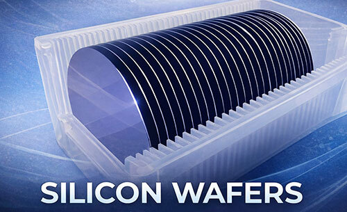
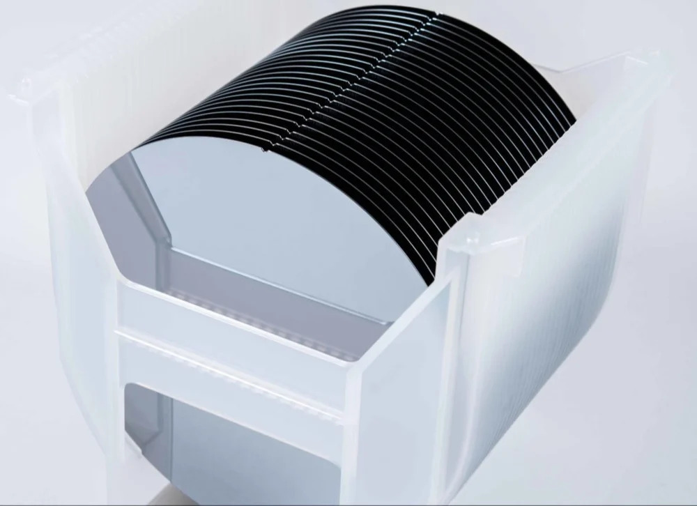
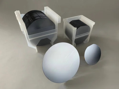
About Industrial Silicon Wafers
Experience the astonishing performance of our hot-selling Industrial Silicon Wafers, designed to meet the demands of advanced semiconductor manufacturing. Boasting valiant precision with crystal orientation options (<100>, <111>, <110>), ultra-flat double-sided polished surfaces, and classic monocrystalline purity, these wafers guarantee low defect density (<100/cm2) and superior flatness (5 m TIR). Available in diameters from 100 mm to 300 mm and compatible with both P-type and N-type doping, they withstand temperatures up to 1100C. Take advantage of their high accuracy (0.01 mm thickness tolerance) and Class 10 cleanroom processing. Perfect for solar cell, IC, and semiconductor production. Vacuum-sealed, edge options, and secure delivery across India from a reputed manufacturer, supplier, and trader.
Astonishing Material & Remarkable Applications
Crafted from high-purity monocrystalline silicon, our Industrial Silicon Wafers stand out for their ultra-flat surfaces and exceptional temperature resistance. Designed for reliability and precision, these wafers excel in semiconductor fabrication, solar cell production, and integrated circuit manufacturing. Their versatility accommodates P-type or N-type usage, with application-focused dimensions between 100 mm and 300 mm. Valiant in engineering and classic in consistency, these wafers meet industrial demands for high performance and dependability in every use.
Sample Policy & Certifications: Quick and Secure
We provide sample Industrial Silicon Wafers with express shipping to expedite your evaluation process. A nominal expenditure or minimal charge may apply, ensuring you receive high-quality samples promptly. All wafer batches come with verified certifications and adhere to industry-leading cleanliness standards, so you can confidently assess product suitability. Our vacuum-sealed, cleanroom-compatible packaging preserves sample integrity, making our trial policy cost-effective and reliable for potential buyers across India and beyond.
FAQ's of Industrial Silicon Wafers:
Q: How do Industrial Silicon Wafers ensure reliability in semiconductor manufacturing?
A: These silicon wafers are fabricated with monocrystalline purity, ultra-flat surfaces, and a defect density below 100/cm2, ensuring high performance and consistency in semiconductor manufacturing applications.
Q: What are the available crystal orientations and sizes for these wafers?
A: Our wafers come in crystal orientations <100>, <111>, and <110>, with diameters ranging from 100 mm to 300 mm, allowing for broad compatibility with various manufacturing processes.
Q: When can I expect to receive sample wafers after requesting?
A: We offer express shipping for sample wafers and strive for quick turnaround times. Once requested, samples are typically dispatched promptly to minimize waiting periods.
Q: Where are these Industrial Silicon Wafers manufactured and supplied from?
A: All wafers are manufactured, supplied, and traded from India, ensuring easy access and swift support for local and global clients.
Q: What is the process for ordering and receiving certified wafers?
A: Once you place an order, your wafers-processed in a Class 10 cleanroom and vacuum-sealed-are shipped securely. Certification and documentation accompany every batch.
Q: What benefits do P-type and N-type doping provide in these wafers?
A: P-type and N-type doping offer flexibility for different electronic device requirements, enhancing the wafer's adaptability and performance in varied industrial applications.
 Send Inquiry


 Send Inquiry
 English
 Spanish
 French
 German
 Italian
 Chinese (Simplified)
 Japanese
 Korean
 Arabic
 Portuguese