About Lab Silicon Wafer
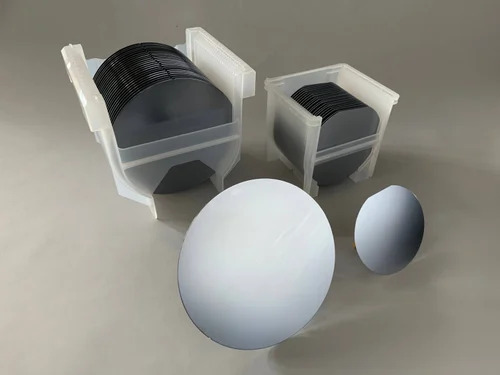
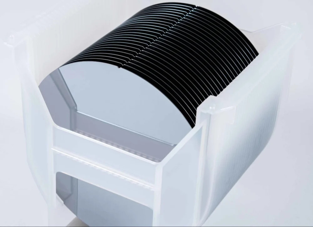
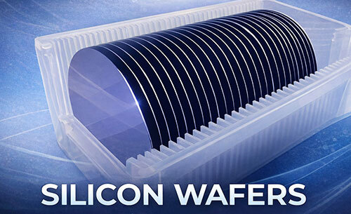
Discover the new release: Lab Silicon Wafer, crafted for researchers who demand peerless quality. Select from N, P, or Intrinsic doping and pick yours in single, double, or unpolished mirror finishes. Our wafers boast prodigious purity-prime grade high-purity silicon for unassailable performance in R&D, microelectronics, and lab use. Stock is readily available with a wafer capacity of 25 per pack; choose sawn or rounded edges, 100mm-200mm diameter, ~525m thickness, and high or low resistivity. Each silicon wafer is an unyielding asset for innovators across India.
Key Features and Usage Areas
This Lab Silicon Wafer exemplifies advanced engineering with mirror surface finish, 100 or 111 orientation, and superior temperature resistance up to 1200C. Its intrinsic and doped options suit a wide spectrum of laboratory, R&D, and microelectronic applications. As a lab consumable, it is engineered for accuracy and consistency, supporting both standard and customizable dimensions. Its high-purity silicon construction ensures optimal results for scientists, innovators, and technology developers.
Supply Capacity and Shipped Goods Details
We maintain an unassailable supply ability with stock always available, shipping 25 wafers per secure package. All goods are wrapped to ensure pristine condition upon arrival. Your order is dispatched promptly, and you can select from various packaging options for added safety. We accept a range of payment terms, providing flexibility for manufacturers, suppliers, and traders. Our supply chain ensures your silicon wafer requirements are met seamlessly across India.
FAQ's of Lab Silicon Wafer:
Q: How are the Lab Silicon Wafers packaged for shipment?
A: Lab Silicon Wafers are securely packaged in protective containers, with each pack containing 25 wafers to prevent damage during transportation and to maintain their mirror surface quality.
Q: What is the process for selecting wafer specifications?
A: You can select your preferred specifications such as doping type (N, P, Intrinsic), finish (single, double, unpolished), diameter, thickness, resistivity, and edge style. Customizable options are also available to meet unique requirements.
Q: When can I expect my silicon wafers to be dispatched after ordering?
A: Orders are promptly dispatched as soon as payment is confirmed. With stock always available, shipment is efficiently arranged to reach you in the shortest possible time.
Q: Where are these silicon wafers manufactured and supplied from?
A: The Lab Silicon Wafers are manufactured, supplied, and traded from India, ensuring swift delivery for domestic orders and adherence to international standards.
Q: What type of laboratory and industrial applications are these wafers suitable for?
A: These wafers are suitable for laboratory research, R&D projects, and microelectronics manufacturing due to their high purity, temperature resistance, and customizable features.
Q: How does the high-purity, prime grade silicon benefit my research?
A: Using prime grade, high-purity silicon ensures reliability, low contamination, and unassailable performance, which are critical for high-precision laboratory experiments and technology development.
 Send Inquiry


 Send Inquiry
 English
 Spanish
 French
 German
 Italian
 Chinese (Simplified)
 Japanese
 Korean
 Arabic
 Portuguese